Infineon Interview: Third-generation semiconductors and silicon devices will coexist for a long time
Similarities: Compared to traditional silicon materials, third-generation semiconductor materials represented by silicon carbide (SiC) and gallium nitride (GaN) have larger bandgap widths and higher critical field strengths, giving power semiconductors made from these two materials excellent characteristics such as high voltage resistance, low on-resistance, and low parasitic parameters.
Differences and their respective applications: There are also many differences between silicon carbide and silicon nitride, two wide bandgap semiconductor materials.
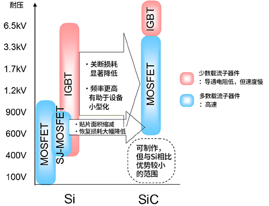
Different applicable voltage and other characteristics have different target applications: Silicon carbide is suitable for a voltage range of 650 V to 3.3 kV, making it a high-frequency device above 1200V. It also features high power density and has a wide range of applications, such as solar inverters, new energy vehicle charging, rail transit, high-speed air compressors in fuel cells, DCDC and electric vehicle motor drives, and data centers under the digital trend. These will all become application markets for silicon carbide. Infineon supplies silicon carbide products to over 3,000 customers in these markets.
Compared to silicon carbide, gallium nitride is suitable for a lower voltage range, from medium voltage 80 V to 650 V. However, it features fast switching frequencies, with gallium nitride switching frequencies reaching the MHz level, making it suitable for medium-power applications with the highest switching frequencies, such as fast charging and data centers.
SiC/GaN growth outlook: Overall, the silicon carbide market is experiencing strong growth. Initially, demand was mainly driven by industrial applications such as solar energy and electric vehicle charging, but now, this demand is increasingly being surpassed by the high demand for automotive applications. Another very promising semiconductor material is gallium nitride. For example, in the field of compact, high-performance, and especially efficient charging systems—such as chargers for consumer devices and power supplies for telecommunications equipment—its advantages are particularly evident. The gallium nitride market is also expected to experience rapid growth: from $47 million (2020) to $801 million (2025) (CAGR: 76%).
Infineon's main products: Compared to competitors, Infineon's advantage lies in its possession of three major power semiconductor technologies—silicon, gallium nitride, and silicon carbide—and has accumulated extensive experience in semiconductor design, production, and various application fields. This enables us to be fully customer-oriented and provide outstanding products and solutions to meet customers' unique application requirements.
02
With the continuous advancement of the dual carbon policy, what new competitive advantages can third-generation semiconductors bring to related systems in terms of energy saving and efficiency improvement? What solutions does your company have related to third-generation semiconductor power devices that can help improve system energy efficiency?
Entering the post-Moore's era, on one hand, human society is pursuing improvements in quality of life through technologies such as the Internet of Everything, artificial intelligence, big data, smart cities, and intelligent transportation, accelerating its pace of development. On the other hand, improving global climate conditions through low-carbon living is becoming a growing consensus.
Currently, about one-third of global energy demand comes from electricity. The growing energy demand, the depletion of fossil fuel resources, and issues like climate change require us to seek smarter and more efficient ways to produce, transmit, distribute, store, and use energy.
Throughout the entire energy conversion chain, the energy-saving potential of third-generation semiconductor technology can make a significant contribution to achieving long-term global energy-saving goals. In addition, wide bandgap products and solutions help improve efficiency, increase power density, reduce size, reduce weight, and lower overall costs, thus contributing to energy efficiency improvements in a wide range of application scenarios such as transportation, new energy power generation, energy storage, data centers, smart buildings, home appliances, and personal electronic devices.
For example, in power electronics applications, high-speed power devices with voltage tolerances above 1200V have long been anticipated, and today, SiC MOSFETs are the top choice.
In addition to high speed, silicon carbide also features high thermal conductivity, high breakdown field strength, and high saturation electron drift rates, making it especially suitable for applications requiring harsh conditions such as high temperature, high power, high voltage, high frequency, and radiation resistance.
Power density is another important aspect of device technology. SiC MOSFET chips have much smaller areas than IGBTs; for example, a 100A 1200V SiC MOSFET chip is about one-fifth the size of the IGBT and freewheeler diodes combined. Therefore, in motor drive applications, the value of SiC MOSFETs is well realized, including 650V SiC MOSFETs.
In terms of high-voltage resistance, SiC high-speed devices above 1200V can improve system performance and power density by increasing the system's switching frequency. Here are two examples:
a) As high-voltage, high-speed, high-current devices, silicon carbide devices simplify the circuit structure of DC pile charging modules, increase unit power ratings, and significantly increase power density, paving the way for reducing system costs for charging piles.
For the power unit of an electric vehicle DC charging station, if a Si MOSFET is used, two channels are connected in series, whereas with a SiC MOSFET, a single channel can be achieved, greatly increasing the power of the charging station's single unit.
Using Infineon's single silicon carbide tube, the charging module's power can reach over 30 kilowatts. Using Infineon's silicon carbide modules, the charging module's power can reach over 60 kilowatts. The design of MOSFET/IGBT single-tube tubes is still at the 15-30 kW level.
b) Flyback auxiliary power supply in three-phase systems, with a 1700V SiC MOSFET, is also a perfect solution.
In terms of reliability and quality assurance, SiC devices come in two types: planar gate and trench gate. Infineon's trench-gate SiC MOSFETs effectively avoid the reliability issues of the flat gate oxide layer while also offering higher power density.
Thanks to these outstanding performances, SiC MOSFETs have applications in photovoltaic inverters, UPS, ESS, electric vehicle charging, fuel cells, motor drives, and electric vehicles.
However, will silicon carbide become the ultimate solution for all-encompassing applications?
As is well known, silicon-based power semiconductors are the main representatives— — IGBT technology has encountered some difficulties in further improving performance. Switching losses and reduced saturation voltage drop on each other constrain each other, leaving less room for loss reduction and efficiency improvement. As a result, the industry hopes that SiC can become a disruptive technology. However, this view is not very comprehensive. First, silicon-based IGBT technology represented by Infineon is also advancing. With advances in packaging technology, the performance and power density of IGBT devices are increasing. At the same time, products developed for different applications can undergo special optimizations to improve the performance of silicon devices in the system, thereby enhancing system performance and cost-effectiveness. Therefore, the development of third-generation semiconductors will inevitably go hand in hand with silicon devices. Alongside technological advancement, there are also considerations of large-scale commercial value factors for different applications. It is unrealistic to expect third-generation devices to quickly replace silicon devices in all application scenarios.
03
With new energy vehicles and charging piles also becoming one of the main application areas for third-generation semiconductors, what do you think are the main technical advantages of third-generation semiconductors in these two areas? What new improvements and new application possibilities can it bring to system efficiency and performance?
New Energy Vehicles:
In new energy vehicle-related fields, range and battery capacity are key. SiC technology can significantly improve driving range or reduce battery installation and cost at the same range. Therefore, SiC is being adopted more and more, especially in traction main inverters, onboard charger OBC, and high and low voltage DC-DC converters.
Technical advantages SiC brings to the above applications:
Traction main inverter:
Increase battery utilization by more than 5%
Higher power density can reduce system size
Lower conduction losses under light load
Lower switching losses than silicon-based IGBTs
Lower cooling requirements and fewer passive components reduce system costs
Onboard charger OBC and DCDC:
Faster switching speeds help reduce passive components, thereby increasing power density or achieving smaller sizes.
CoolSiC™ Automotive-grade MOSFETs have the industry's lowest switching losses under high-speed switching conditions
In the PFC and DC-DC stages, onboard charger efficiency can be improved by 1%, resulting in lower cooling requirements.
The totem pole topology supports bidirectional charging
It is important to emphasize that in the coming years, different semiconductor technologies will coexist in the market, each offering unique advantages in different application scenarios. In traction inverters, SiC and silicon-based IGBTs each have their own opportunities based on different mileage, efficiency, and cost considerations. For example, SiC is used for rear wheel main traction drive, which can increase cruising range; Silicon-based IGBTs are used for the front wheels to optimize costs. In extreme cases, such as in on-board chargers, up to five different semiconductor technologies can be used simultaneously within the same architecture, including IGBT, silicon-based diodes, silicon-based MOSFETs, superjunction MOSFETs, and SiC MOSFETs.
Infineon's layout in automotive-grade silicon carbide products:
Infineon has launched a wide range of SiC solutions and a comprehensive automotive-grade product line for various xEV systems, including CoolSiC & trade; Automotive diodes, CoolSiC & trade; Hybrid PACK & trade for automotive MOSFETs and full SiC modules; Drive CoolSiC™ and more.
Recently, in March 2021, we released the 650V CoolSiC & trade, which offers industry-leading switching and conduction losses; Hybrid discrete devices. Compared to silicon devices, it offers higher scalability and has been widely used in multiple vehicle models. This device perfectly aligns with the trend of bidirectional charging with ideal cost-performance in a totem pole topology.
In May, Infineon released HybridPack-Drive CoolSiC for traction inverters; Products. The HybridPack-Drive series has shipped over one million units and is used on more than 20 automotive platforms worldwide. New Hybrid Pack - Drive CoolSiC ™ The product is the first module on the market to pass automotive-grade certification, offering strong scalability compared to corresponding silicon devices, easily covering the 180kW power range. This product is based on our improved trench gate MOSFET technology, featuring both high reliability and high performance. This product can be used in 800V battery systems, offers two selectable current levels, and has already been deployed on Hyundai's new Ioniq 5 model on the 800V e-GMP platform.
Infineon's Si and SiC product lines both offer high scalability, which is a key feature that sets us apart from other brands. Users can freely choose different packages, voltage levels, and power levels from our Si and SiC product lines as needed, achieving high design flexibility, accelerating product time-to-market, and reducing design difficulty. This feature is a highly valued consideration by customers in fast-changing markets such as electric vehicles. Additionally, the high-efficiency features of our products help customers achieve their design goals of improving electric vehicle driving range.
04
Data centers are an important application area for energy saving and consumption reduction. In what ways do you think third-generation semiconductors can improve the energy efficiency of data centers? In data centers, which third-generation semiconductor products can be widely applied? How will the application of third-generation semiconductors affect the upgrade of data center functions?
In fact, data centers consume a lot of energy. In 2021, electricity consumption was about 93.7 billion kWh. In other words, most of the energy consumption actually comes from IT equipment consumption, but the entire power supply transmission and distribution structure also determine the energy efficiency of the entire data center. Therefore, we see a new trend that may shift from the current traditional UPS distribution structure to an integrated power supply system with power electronic transformers (SST) as the main interface, essentially a DC power supply system.
Based on silicon carbide technology, this power electronic transformer can directly convert 10 kV of mains electricity into 380 V DC. Based on current cases already in use, power supply efficiency can be improved to over 95%, and DC distribution network efficiency can also be improved to over 97%. Therefore, it is believed that in this field, there will be more significant development and validation in 2022. Throughout this process, we are also very much looking forward to using Infineon's advanced silicon carbide technology to ensure the continuity and security of power supply in data centers.
05
With the promotion and application of third-generation semiconductor materials, gallium nitride is not only rapidly capturing the market in fast charging, but in which other areas may it emerge in the future? What products and solutions does your company offer?
Changes in the GaN market: In the past two years, the commercialization of silicon-based GaN switchgear has changed significantly compared to the general market view five years ago, notably the rapid growth of high power density fast charging based on GaN components. This shows that technology is just one of many factors influencing the development of the new materials market. In the next five years, the application areas of gallium nitride that we are optimistic about include: consumer fast charging, server/communication power supplies, motor drivers, industrial power supplies, audio equipment, wireless charging, LiDAR, etc. Among these, fast charging will continue to lead the growth of the GaN switching device market.
Technical challenges in the implementation of GaN and Infineon's solution: As a power switching device, silicon-based GaN is being commercialized, and besides performance and price, the most concerning topic is long-term reliability. Currently, the vast majority of GaN switching devices grow GaN on silicon substrates and use two-dimensional electron gas as the channel, using GaN HEMTs. Since IR released the industry's first silicon-based GaN switchgear in 2010, research on silicon-based GaN has become quite in-depth, but truly large-scale application has only emerged in recent years. Relatively speaking, silicon and even silicon carbide have been in the market for much longer and have a much larger number of existing devices, so compared to the other two materials, gallium nitride has far fewer failure cases available for analysis. This is one of the reasons why fast-charging consumer products have become the rapid growth engine for gallium nitride. Additionally, the ultra-low parasitic parameters of silicon-based GaN not only offer users extremely low switching losses but also greatly increase the difficulty of driving such devices.
Infineon was early on focused on the reliability of silicon-based GaN research and added multiple measures beyond the JEDEC standard to ensure the long-term reliability of the silicon-based GaN we produce far exceeds the market average. Additionally, the long-term reliability of silicon-based GaN is highly related to the device's voltage swing, switching frequency, duty cycle, temperature, and so on in its application scenarios. Therefore, we recommend that users engage in in-depth discussions with technical support personnel of silicon-based GaN suppliers during product design on specific application scenarios to assess long-term reliability. In terms of device driving, Infineon has developed dedicated gallium nitride drivers to reduce the pressure on users when designing driver circuits.
06
As this wave of chip shortages gradually subsides, we can see that there are many areas in the chip supply chain that need improvement. So, how will third-generation semiconductors optimize their supply chain? How can power semiconductor companies address issues in the materials supply chain?
Today, Infineon leads the industrial application market for SiC and successfully drives the use of SiC in the automotive sector with the industry's broadest and most scalable product portfolio. The company supplies more than 3,000 customers directly or through distribution. For over 20 years, silicon carbide (SiC) has been very important to Infineon. As early as 2001, we launched SiC-based products and solutions on the market.
At Capital Markets Day last October, Infineon presented its outlook for its silicon carbide and gallium nitride (GaN) business. Infineon expects its silicon carbide business to grow by 90% this fiscal year, with sales reaching $1 billion and a 30% market share by around 2025.
To ensure supply reliability, Infineon relies on an extensive supplier network and joint efforts with various partners.
Infineon also announced plans to invest over 2 billion euros to establish a plant in Külin, primarily producing compound semiconductors. We will continue to expand production capacity at Villach.
In 2018, Infineon strategically acquired Siltectra's wafer and ingot cutting technology, significantly reducing raw material waste in SiC production to increase output and thereby enhance our competitive edge.
07
So, as costs decrease, do you think GaN can fully replace silicon-based power devices such as diodes, IGBTs, and MOSFETs in the mid- and low-power fields in the future? What changes have third-generation semiconductors brought about in power device processes?
At least in the foreseeable future, third-generation semiconductors will not completely replace first-generation semiconductors. From a cost-performance perspective, silicon-based semiconductors remain the best choice across a wide range of applications. The current bottleneck for commercialization of third-generation semiconductors is the high cost. Although it is declining rapidly, it is still far higher than silicon-based semiconductors.
Of course, we may see some third-generation semiconductor devices priced close to silicon-based semiconductors on the market, but that doesn't mean their cost is close to silicon-based semiconductors. That's a business move, using low pricing to stimulate the market. At present, the cost of third-generation semiconductors is still much higher than that of silicon-based semiconductors.
In the foreseeable future, silicon-based semiconductors will still occupy the majority of the market. Silicon carbide is mainly used in high-power, high-voltage scenarios. GaN is mainly used in scenarios that require ultra-high frequencies, with fast charging in smartphones being a notable example.
Source: Electronics World Author: Infineon Technology