Characteristics of SiC-MOSFETs and their differences from Si-MOSFETs and IGBTs
Transistors play a crucial role in power conversion circuits, and various improvements have been made to further achieve low loss and compact application sizes. The advantages of SiC power device semiconductors have already been introduced earlier, such as low loss, high-speed switching, and high-temperature operation. It is clear that these advantages are very useful. This chapter will further deepen our understanding of SiC-MOSFETs by comparing them with other power transistors.
Features of SiC-MOSFETs
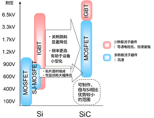
A similar diagram is also used in the SiC-SBD chapter to introduce the withstand voltage coverage range. Similarly, this figure shows the voltage withstand range of SiC-MOSFETs by comparing them with Si power devices.
Currently, the effective range of SiC-MOSFETs is rated above 600V, especially above 1kV. Regarding advantages, let's compare products above 1kV with the current mainstream Si-IGBTs. Compared to IGBTs, SiC-MOSFETs reduce losses when switching off, enabling high-frequency operation and helping to miniaturize applications. Compared to SJ-MOSFETs (Super Junction MOSFETs) with the same voltage tolerance, the on-resistance is lower, which can reduce the chip area of the same on-resistance and significantly decrease recovery losses.
The table below summarizes the characteristics of power components rated at 600V~2000V.
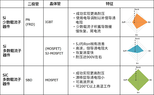
In radar diagrams, RonA is the on-resistance per unit area (representing the loss during conduction), BV is the component withstand voltage, Err is the recovery loss, and Eoff is the loss from the off-switch switch. SiC is already very perfect, and in the current comparison, it is by no means overestimated.
The next article will provide a more detailed introduction to the features of SiC-MOSFETs, combining comparisons with SJ-MOSFETs and IGBTs.
Comparison of the structure and characteristics of power transistors
Continuing from the previous section, we will continue with the comparison of various power transistors. This article compares structure and characteristics.
Comparison of the structure and characteristics of power transistors
The diagram below compares the structure, voltage rating, on-resistance, and switching speed of each power transistor.
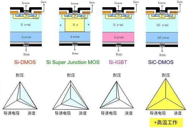
Different process technologies and structures differ, resulting in different electrical characteristics. To clarify, DMOS is a planar MOSFET and is a common structure. Si power MOSFETs, due to their high voltage tolerance and ability to reduce on-resistance, have recently become popular in MOSFETs with super junction structures (hereinafter referred to as SJ-MOSFET” ) is being used more and more widely. Regarding SiC-MOSFETs, the DMOS structure is presented here, but ROHM has already begun mass production of trench-type SiC-MOSFETs with superior characteristics. Details will be introduced later.
In terms of characteristics, Si-DMOS faces challenges in on-resistance resistance; as mentioned earlier, the on-resistance is improved by adopting an SJ-MOSFET structure. IGBTs perform excellently in terms of on-resistance and voltage rating, but face challenges in switching speed. SiC-DMOS performs excellently in voltage resistance, on-resistance, and switching speed, and it also performs well under high-temperature conditions, making it a highly advantageous switching device.
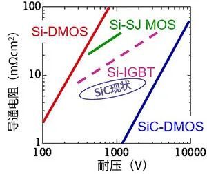
This chart shows the standardized on-resistance and withstand voltage of each transistor. From the figure, it can be seen that theoretically, SiC-DMOS has higher voltage tolerance and can be used to manufacture transistors with low on-resistance. Currently, the current characteristics of SiC-DMOS are defined by an ellipse. With future development, performance is expected to improve further.
Starting from the next article, we will introduce a separate comparison with SiC-MOSFETs.
Differences between SiC-MOSFET and Si-MOSFET
Starting with this article, we will compare SiC-MOSFETs with other power transistors one by one.
This article will introduce the differences from Si-MOSFETs. For those who have never used SiC-MOSFETs, rather than studying each parameter in detail, it is better to first understand the differences between driving methods and Si-MOSFETs. Here, we introduce two key points to note when comparing SiC-MOSFET drivers with Si-MOSFETs.
Difference from Si-MOSFET: Driving voltage
Compared to Si-MOSFETs, SiC-MOSFETs have lower drift layer resistance and higher channel resistance, resulting in higher drive voltage—that is, the higher the gate-source voltage Vgs—the lower the on-resistance. The figure below shows the relationship between the on-resistance of a SiC-MOSFET and Vgs.
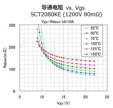
The on-resistance starts to vary (decreases) from about 20V Vgs, then gradually decreases to near its lowest value. The typical IGBT and Si-MOSFET drive voltages are Vgs=10~15V, while SiC-MOSFETs are recommended to drive around Vgs=18V to fully achieve low on-resistance. In other words, one difference between the two is that the driving voltage is higher than that of Si-MOSFETs. When replacing with Si-MOSFETs, it is also necessary to explore gate driver circuits.
Difference from Si-MOSFETs: internal gate resistance
The internal gate resistance Rg of the SiC-MOSFET device itself (chip) depends on the thin-layer resistance of the gate electrode material and the chip size. If the design is the same, it is inversely proportional to chip size; the smaller the chip, the higher the gate resistance. With the same capability, SiC-MOSFET chips are smaller than Si components, resulting in smaller gate capacitance but increased internal gate resistance. For example, 1200V 80mΩ The internal gate resistance of the product (S2301 is a bare chip product) is approximately 6.3 Omega.
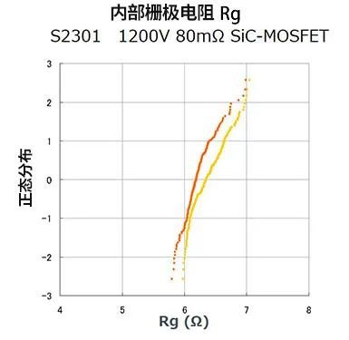
This is not limited to SiC-MOSFETs; the switching time of a MOSFET depends on the combined gate resistance of the external gate and the internal gate resistance introduced above. The internal gate resistance of SiC-MOSFETs is higher than that of Si-MOSFETs, so to achieve high-speed switching, the external gate resistance needs to be as small as possible, down to a few Omegas; Left and right.
However, the external gate resistor also serves to counteract surge applied to the gate, so a good balance with surge protection must be carefully maintained.
Differences from IGBT
The previous chapter focused on the differences from Si-MOSFETs and introduced two key points about SiC-MOSFET driver methods. This chapter will introduce the differences from IGBTs.
Difference from IGBT: VD-ID characteristics
The VD-ID characteristic is one of the most fundamental characteristics of a transistor. Below are the Vd-Id characteristics at 25°C and 150°C.
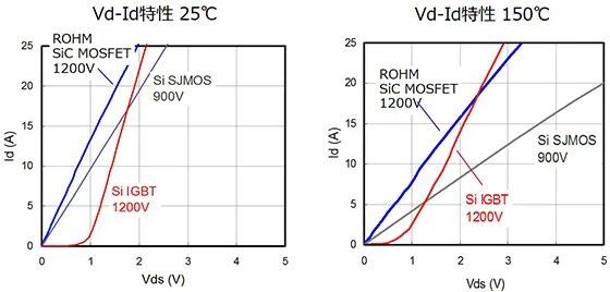
Please see the characteristic chart at 25°C. The Id of SiC and Si MOSFETs increases linearly relative to Vd (Vds), but because IGBTs have a rise voltage, the Vds of MOSFET components are lower in the low current range (for IGBTs, this is collector current and collector-emitter voltage). It goes without saying that the Vd-Id characteristic is also a conduction resistance characteristic. According to Ohm's law, relative to Id, the lower the Vd, the smaller the on-resistance; the steeper the slope of the characteristic curve, the lower the on-resistance.
The low Vd (or low Id) range of IGBTs (in this case, the range from Vd to about 1V) is negligible in IGBTs. This does not pose a problem in high-voltage, high-current applications, but when the power demand of electrical equipment ranges widely from low to high power, the efficiency of the low-power range is not high.
In contrast, SiC MOSFETs can maintain low on-resistance over a wider range.
Additionally, compared to Si MOSFET characteristics at 150°C, the slope of the characteristic curves of SiC and Si-MOSFETs slows down, resulting in increased on-resistance. However, SiC-MOSFETs show very little variation at 25°C, while products with similar characteristics at 25°C have larger differences, and the on-resistance changes little at higher temperatures.
Difference from IGBT: Turn-off loss characteristics
As mentioned several times earlier, SiC power devices have excellent switching characteristics, capable of handling both high power and high-speed switching. Here, we will specifically explain the differences from IGBT switching loss characteristics.
As is well known, when the IGBT switches OFF, tail current flows through the component structure, so increased switching losses are a fundamental characteristic of IGBTs.
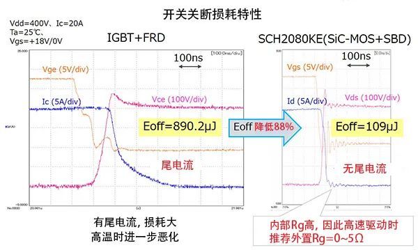
Comparing the waveform when switching OFF, it can be seen that SiC-MOSFETs do not flow through tail current, so the corresponding switching losses are very small. In this case, the SiC-MOSFET+SBD (Schottky barrier diode) combination reduces the turn-off loss Eoff by 88% compared to IGBT+FRD (fast recovery diode).
Another important point is that the tail current of the IGBT increases with temperature. By the way, high-speed driving of SiC-MOSFETs requires appropriate adjustment of the external gate resistor Rg. This was mentioned earlier." Differences from Si-MOSFETs" This has also been mentioned in the media.
Difference from IGBT: conduction loss characteristics
Next, let's look at the losses during switching-on conduction.
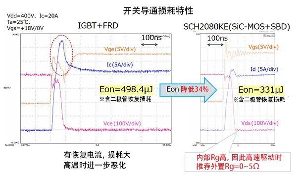
When the IGBT switches on, the current flows through the Ic (blue curve) circled by a red dashed line. This is mostly caused by the diode's recovery current, which is a major loss when switching on. Remember: when using SiC-SBCs in parallel, combined with the fast recovery characteristics, losses during MOSFET switching conduction are reduced; The switching conduction loss when FRDs are paired, like the tail current of the IGBT, increases with temperature.
In summary, regarding switching loss characteristics, it is clear that SiC-MOSFETs outperform IGBTs.
Additionally, the data provided here is based on results under ROHM trial environments. Different conditions such as the driver circuit may also result in different outcomes.
Characteristics of body diodes
The previous chapter covered the differences from IGBT. This chapter will explain the forward and reverse recovery characteristics of SiC-MOSFETs in bulk diodes.
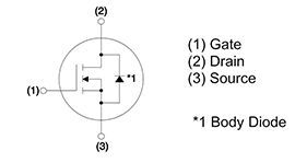
As shown in the figure, MOSFETs (not limited to SiC-MOSFETs) have a body diode between the drain and the source. Structurally, a MOSFET is formed by a pn junction between the source and drain, also known as Parasitic diode Or" Internal diode." For MOSFETs, the performance of the body diode is one of the key parameters, and its performance plays a crucial role in applications.
Forward characteristics of SiC-MOSFET body diodes
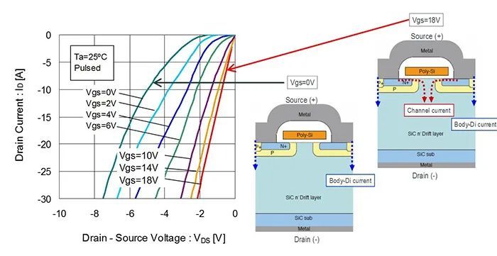
The figure below shows the Vds-Id characteristics of the SiC-MOSFET. In SiC-MOSFETs, a negative voltage is applied to the drain based on the source, and the bulk diode is forward biased. In this figure, the green curve of Vgs=0V basically represents the Vf characteristic of the out-of-body diode. Vgs is 0V, meaning the MOSFET has no channel current in the off state. Therefore, under these conditions, the Vd-Id characteristic can be considered the Vf-If characteristic of the body diode. For example, " What is silicon carbide? SiC has a wider bandgap, and Vf is much larger than that of Si-MOSFETs.
When a 18V voltage is applied between the gate and source and the SiC-MOSFET conducts, the channel section with lower resistance (rather than the body diode section) receives current at the dominant low. To facilitate understanding of various states from a structural perspective, below is a cross-sectional diagram of a MOSFET.
Reverse recovery characteristics of SiC-MOSFET body diodes
Another important characteristic of MOSFET body diodes is the reverse recovery time (trr). trr is an important parameter related to diode switching characteristics, which has also been explained in the article on SiC Schottky barrier diodes. It goes without saying that the bulk diode of a MOSFET is a diode with a pn junction, so reverse recovery occurs, characterized by reverse recovery time (TRR). Below is a comparison of the trr characteristics of the 1000V rated Si-MOSFET and SiC-MOSFET SCT2080KE.
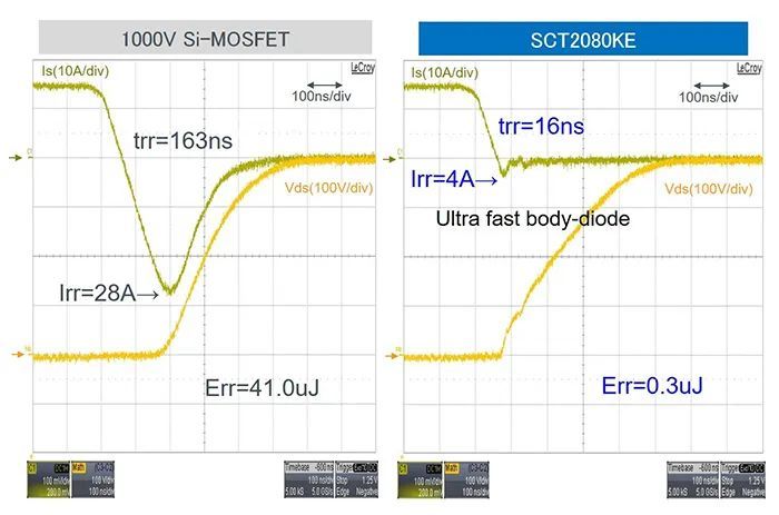
As shown in the figure, the sample Si-MOSFET has a slower trr and flows through a larger Irr. In contrast, the body diode speed of SiC-MOSFET SCT2080KE is extremely fast. TRR and IRR are both nearly negligible levels, and recovery loss Err has been significantly reduced.
Application examples of SiC-MOSFETs
This chapter will introduce some application examples of SiC-MOSFETs. It also includes some previous information and prototype-level content, and hopefully these introductions will help everyone understand the benefits of adopting SiC-MOSFETs and the new functions that can be realized. In addition to SiC-MOSFETs, you can also learn about application examples of SiC-SBD and full SiC modules here.
SiC-MOSFET Application Example 1: Phase-shifting DC/DC converter
Below is the demo device, jointly produced with Power Assist Technology Ltd.
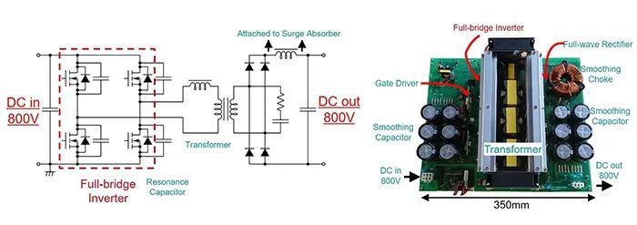
The full-bridge inverter section uses three types of transistors (Si IGBT, second-generation SiC-MOSFET, and the third-generation trench structure SiC-MOSFET introduced in the previous chapter) to form a phase-shifting DCDC converter of the same size, serving as a demonstration unit for comparing product efficiency.
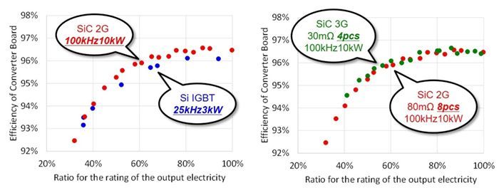
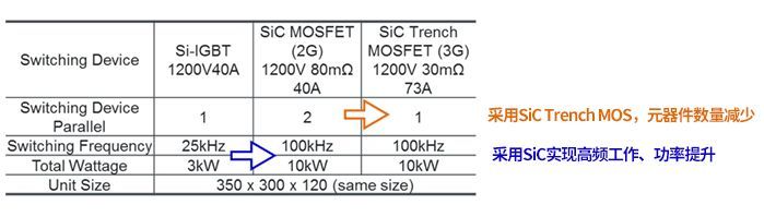
First, in the SiC-MOSFET composition, the advantages of switching performance are leveraged to achieve 100kHz high-frequency operation and power boost, which is difficult for Si IGBTs to achieve. Additionally, in the second-generation (2G) SiC-MOSFET, two transistors are connected in parallel to form a single switch, but the third-generation (3G) SiC-MOSFET has lower on-resistance, reducing the number of transistors from eight to four. Regarding efficiency, the results are most ideal when using third-generation (3G) SiC-MOSFETs, with all SiC-MOSFETs exceeding Si IGBTs in efficiency.
SiC-MOSFET Application Example 2: Pulse Power Supply
Pulse power supplies are systems that provide instantaneous power in a short period, with applications including gas lasers, accelerators, X-rays, plasma power supplies, and so on. Existing solutions include thyristors and other vacuum tubes and Si switches, but the market demands switches with higher voltage tolerance and higher speed. To meet this market demand, the high voltage and high-speed performance of SiC are utilized to achieve ultra-high voltage and high-speed switching. From the perspective of high speed, this is something Si IGBTs find difficult to achieve. The example below is a product developed in collaboration with Fukushima SiC Application Technology Research Co., Ltd., Kyoto New-Tronics Co., Ltd., and the Japan Science and Technology Agency, exhibited at CEATEC 2014 and TECHNO-FRONTIER2015.
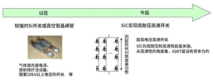
・Ultra-high voltage pulse power supply
Features
・Ultra-high voltage resistance pseudo-N channel
SiC MOSFET
・Low on-resistance
(Less than 1/100 of previous products)
・High repetition rate
Application example
・Charged particle accelerator
・Power supply for medical equipment
・Plasma generators, etc
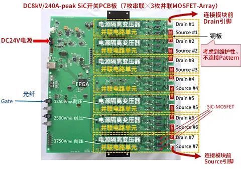
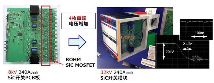
・1~10kV random pulse generator: 13.2kV SiC switch
Source: techclass.rohm